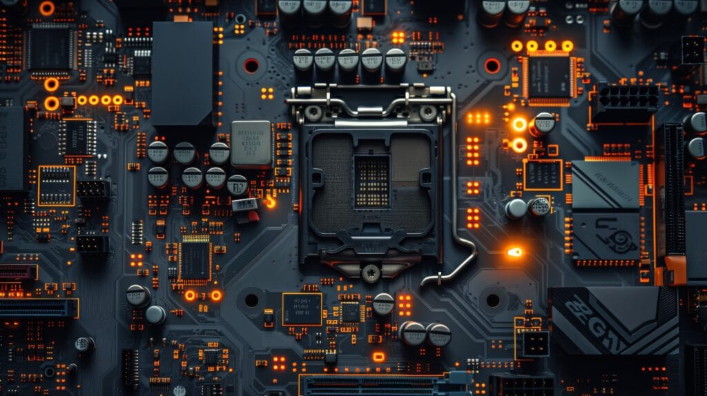
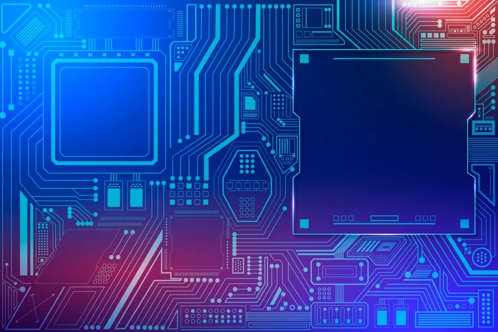
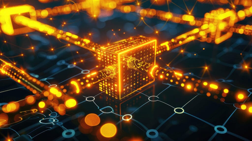
Field Programmable Gate Arrays are at the heart of many modern electronic systems, offering a flexible and reconfigurable platform for custom digital designs.
Unlike fixed-function chips, they can be programmed to perform a wide variety of tasks, making them ideal for applications ranging from signal processing to artificial intelligence.
To truly appreciate their power, it is important to understand the core components of an FPGA and how they work together to create a versatile architecture.
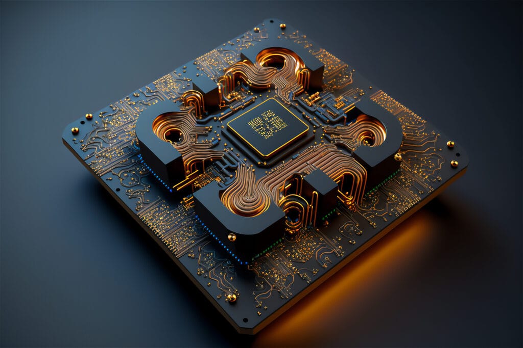
Introduction to FPGA Architecture
It is a semiconductor device that can be configured after manufacturing to implement specific digital circuits.
Its architecture is made up of programmable logic elements, routing resources, and input/output interfaces.
These building blocks enable engineers to design hardware that can be updated or reprogrammed even after deployment, providing unmatched flexibility compared to traditional ASICs.
Logic Blocks
Logic blocks form the computational backbone of an FPGA. Each logic block typically contains look-up tables, flip-flops, and multiplexers.
- Look-up Tables (LUTs) store predefined logic functions that determine how input signals are transformed into outputs.
- Flip-Flops provide memory elements to store data and manage sequential logic.
- Multiplexers help direct signals and allow for different logic configurations.
By combining these elements, logic blocks can implement a wide range of functions, from simple gates to complex arithmetic operations. The ability to customize logic at this level gives FPGAs their unique adaptability.
Routing Resources
For the FPGA to function, logic blocks must communicate with each other. This is where routing resources come in.
These programmable interconnects link logic blocks, memory, and other elements. The routing architecture consists of switch matrices and wiring channels that can be configured to establish the required signal paths.
Efficient routing is critical for achieving high performance and low latency in their designs.
Memory Elements
FPGAs include different types of memory such as block RAM and distributed RAM.
- Block RAM (BRAM) is used for storing larger datasets and implementing buffers or FIFOs.
- Distributed RAM is built from logic resources and is ideal for smaller, faster storage needs.
Memory elements allow designers to build complex data processing pipelines and temporary storage within the FPGA fabric.
Digital Signal Processing Blocks
Many FPGAs include dedicated DSP blocks to handle high-speed arithmetic operations such as multiplication and accumulation.
These blocks are optimized for tasks like image processing, wireless communication, and machine learning inference, reducing the need for external components and improving overall efficiency.
Input and Output Interfaces
The I/O blocks form the communication bridge between the FPGA and external devices. They support a wide range of standards including LVDS, PCIe, and Ethernet.
Each I/O block can be configured for specific voltage levels and signal types, ensuring seamless integration with sensors, processors, and peripheral hardware.
Proper I/O configuration is essential to maintain signal integrity and meet system requirements.
Clock Management
Precise timing is vital in digital systems. FPGA devices incorporate clock management resources such as phase-locked loops and clock distribution networks.
These components ensure that signals are synchronized across the design and help achieve reliable operation even in high-speed applications.
Advantages of FPGA Architecture
The modular architecture of FPGAs offers a wide range of benefits that make them indispensable in modern system design and development:
- Flexibility and Reconfigurability– Unlike fixed-function hardware, they can be reprogrammed to adapt to new requirements, updated standards, or changing customer needs without the cost and time of fabricating new silicon. This makes them highly valuable in industries where technology evolves rapidly.
- Parallel Processing for High Performance– They can execute multiple operations at the same time through their parallel architecture. This enables faster data handling, lower latency, and improved performance compared to sequential processing in traditional processors. Applications such as AI acceleration, real-time analytics, and signal processing benefit heavily from this capability.
- Rapid Prototyping and Iteration– Engineers can design, implement, and test their ideas directly on FPGAs, making it easier to validate concepts quickly. This accelerates time-to-market while reducing risk and cost, since designs can be modified and refined in real time before committing to ASIC or SoC fabrication.
Together, these features make FPGAs a strategic choice for applications ranging from telecom and automotive to aerospace, AI, and high-performance computing.
Conclusion
Understanding the internal structure of an FPGA, from logic blocks to I/O interfaces, reveals why these devices are so powerful and versatile.
By mastering these architectural components, designers can harness the full potential of them to build innovative solutions across industries such as telecommunications, aerospace, automotive, and artificial intelligence.
Whether developing a high-speed signal processing system or a custom computing platform, a solid grasp of FPGA architecture is the first step toward creating efficient and future-ready designs.