FPGAs (Field-Programmable Gate Arrays) play a vital role in the world of digital design, offering unparalleled flexibility and performance. However, designing and debugging FPGA-based systems can be a complex and time-consuming process. Debugging, in particular, is a critical phase that requires careful attention to identify and resolve issues in the FPGA design.
The art of FPGA debugging involves finding and fixing errors, verifying functionality, and optimizing performance. However, traditional debugging approaches can be slow and tedious, often leading to prolonged development cycles and delayed project timelines. To overcome these challenges, it is crucial to employ strategies that speed up the FPGA debugging process.
In this blog post, we will delve into the art of FPGA debugging and explore techniques to enhance its efficiency. We will discuss common FPGA debugging techniques, such as error message analysis, simulation tools, built-in self-test (BIST), and signal observation with logic analyzers. Building upon these foundations, we will then delve into strategies specifically designed to expedite FPGA debugging.
The 20/80 principle for the FPGA design and debugging project
Our experience and that of our colleagues show that modeling and debugging take up most of an FPGA project’s timing. You can focus on Pareto’s law: about 20% of the time is spent on the development itself, writing code, implementing the upper-level design in the form of a block diagram, and about 80% is used for testing, debugging, and support.
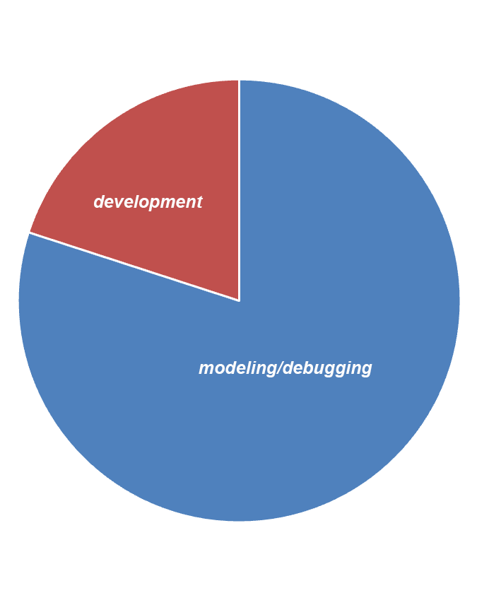
Why do we have this kind of 20/80 ratio?
This is partly due to the iterative development process itself. Each iteration takes a long time, and large projects take a long time to assemble. For example, an hour and a half is a required minimum for the typical Xilinx FPGA project (such as Xilinx Zynq UltraScale+).
There are larger projects that can take much longer to assemble.
To complete the debugging process, a software engineer needs not only the skill of FPGA programming in one of the hardware description languages (HDLs or create its block design) but also programming skills in other languages. For example, C and Python for writing some test scripts. You may also need a scripting language such as Tcl.
Now let’s look at how to shorten the debugging phase, which is the last one in our workflow but takes up the bulk of the project’s time.
Common FPGA debugging techniques include:
Reading and analyzing error messages and warnings is important because FPGA development tools frequently offer thorough error messages and cautions that can help designers spot potential design flaws. Debugging can benefit from an understanding of and analysis of these messages.
Using specialized simulation tools to simulate the FPGA design allows designers to verify the functionality and behavior of the design before implementing it on the actual hardware. This is known as pre-silicon debugging. Early in the development process, this aids in finding and fixing problems.
Using built-in self-test (BIST) and assertion-based verification: Implementing BIST modules within the FPGA design allows for self-testing of specific blocks or modules. Additionally, assertion-based verification involves adding assertions in the design code to verify expected behavior and detect anomalies.
Implementing debug features within the FPGA design: Including dedicated debug features in the FPGA design, such as status registers, counters, or LED indicators, can assist in monitoring and diagnosing issues during runtime.
Observing signals with logic analyzers or oscilloscopes: External tools like logic analyzers or oscilloscopes can be connected to the FPGA to capture and analyze specific signals or waveforms in real-time. This can help identify timing issues, glitches, or unexpected behavior.
Debugging with JTAG and boundary scan: JTAG (Joint Test Action Group) interfaces provide a standardized method for accessing and debugging FPGA designs. Boundary scan techniques enabled through JTAG, allow for testing and debugging of interconnects and I/O pins.
Leveraging vendor-specific debugging tools and resources: FPGA vendors often provide dedicated debugging tools and resources that can assist in diagnosing and resolving issues specific to their platforms. These tools may include features like waveform viewers, on-chip debuggers, or specialized debug IP cores.
Strategies to Speed up FPGA Debugging:
- Writing clean and modular code:
- Well-structured code with clear naming conventions and comments makes debugging easier and faster.
- Utilize design patterns and create reusable modules to reduce duplication and improve code readability.
- Debugging in small increments:
- Break down the FPGA design into smaller functional blocks.
- Test and debug each block individually before integrating them into the larger design.
- This approach helps isolate issues and reduces the scope of debugging.
- Leveraging debugging features of development tools:
- FPGA development environments often provide advanced debugging features.
- Use breakpoints to halt the design execution at specific points and inspect internal signals and variables.
- Utilize watchpoints to monitor changes in specific signals or variables during runtime.
- Take advantage of trace capabilities to analyze the flow of signals and identify issues.
- Effective use of simulation and emulation:
- Utilize simulation tools to identify and fix design issues before synthesizing and implementing the design on the FPGA.
- Simulations allow for faster iterations and provide a controlled environment for debugging.
- FPGA emulators can be used for real-time debugging by running the design on an FPGA-like hardware platform.
- Using hardware debugging techniques:
- Debugging with JTAG (Joint Test Action Group) and boundary scan enables visibility into internal signals and registers.
- JTAG interfaces can be used to halt the design, inspect internal states, and perform interactive debugging.
- Inserting debug logic within the FPGA design allows for runtime debugging without halting the entire design.
FPGA debugging tools
High-level or embedded software engineers have an extensive toolkit: debuggers, the ability to execute program code step-by-step, and extensive program logging capabilities. As for FPGA engineers, they have a limited set of tools to debug their FPGAs. So, what do we have:
- Measuring equipment: oscilloscopes and logic analyzers. These tools allow you to understand what’s going on outside your FPGA, but they don’t let you look inside it. You can use them to debug the external interface and see how the FPGA interacts with the outside world.
- Built-in debugging tools enable you to look inside your FPGA. All popular FPGA manufacturers have such tools with different names: Xilinx, the most popular manufacturer, offers ChipScope, Intel(ex. Altera) has SignalTap, Microchip (ex. Microsemi) uses a product by Synopsys, which is called Identify RTL Debugger. These built-in debuggers are similar in function.

Best Practices for Efficient FPGA Debugging
A. Establishing a structured debugging process
- Documenting and tracking issues: Maintain a centralized system to log and track identified issues, including their descriptions, steps to reproduce, and current status.
- Collaboration and communication among team members: Foster effective communication channels among team members to share debugging insights, progress, and potential solutions.
B. Creating test benches and stimuli
- Designing comprehensive test benches for functional verification: Develop thorough test benches that cover various scenarios and edge cases to validate the functionality of the FPGA design.
- Generating appropriate stimuli to reproduce issues: Craft stimuli that can reliably reproduce the problems encountered during debugging, making it easier to isolate and analyze the root cause.
C. Using assertions and functional coverage
- Adding assertions to check the expected behavior of the design: Integrate assertions within the FPGA code to verify the correctness of certain conditions or behaviors, aiding in detecting anomalies during debugging.
- Ensuring sufficient functional coverage for effective debugging: Develop a comprehensive set of functional coverage goals to ensure that all critical design aspects are tested and debugged adequately.
D. Leveraging vendor-specific debugging tools and resources
- Exploring vendor-provided debugging features and methodologies: Familiarize yourself with the debugging tools and resources offered by the FPGA vendor, such as integrated debuggers, performance analyzers, and profiling tools.
- Tapping into online forums and community support: Engage with the FPGA community and participate in forums or online communities to seek guidance, advice, and solutions from experienced FPGA developers and experts.
E. Utilizing simulation and emulation effectively
- Leveraging simulation tools to identify and fix design issues: Utilize simulation environments to simulate and debug the FPGA design before physical implementation, allowing for faster iteration and debugging cycles.
- Utilizing FPGA emulators for real-time debugging: Utilize FPGA emulators that offer the ability to test and debug the design in real-time, providing a more accurate representation of the final hardware behavior.
F. Using hardware debugging techniques
- Debugging with JTAG and boundary scan: Utilize JTAG interfaces and boundary scan techniques to access internal signals, perform non-intrusive testing, and analyze the behavior of the FPGA at runtime.
- Inserting debug logic within the FPGA design: Incorporate additional debug logic, such as debug registers or probes, into the FPGA design itself to facilitate real-time debugging and observation of critical signals.
G. Continuous integration and automated testing
- Implementing a continuous integration (CI) pipeline: Set up a CI pipeline to automate the testing and debugging process, enabling frequent and consistent testing of the FPGA design as changes are made.
- Employing automated testing frameworks: Utilize automated testing frameworks to streamline the testing and debugging process, reducing human error and ensuring thorough coverage.
H. Conducting code reviews and pair programming
- Performing code reviews: Encourage code reviews within the team to identify potential design issues, improve code quality, and facilitate early detection of bugs.
- Pair programming: Engage in pair programming activities, where two developers work together on the same task, promoting knowledge sharing, brainstorming, and faster problem-solving during debugging.
Conclusion
Efficient FPGA debugging is essential for FPGA designers to enhance productivity and deliver high-quality designs. This article provided practical strategies to speed up the debugging process. We explored common debugging techniques and discussed approaches such as writing clean code, debugging in small increments, utilizing development tools, leveraging simulation and emulation, and employing hardware debugging techniques.
By establishing a structured debugging process, creating comprehensive test benches, using assertions, and tapping into vendor-specific resources, designers can optimize their debugging workflow. Real-world case studies showcased the effectiveness of these strategies.
Mastering the art of FPGA debugging empowers designers to save time, reduce time-to-market, and improve design performance and reliability. Embracing efficient debugging techniques unlocks the full potential of FPGA technology.