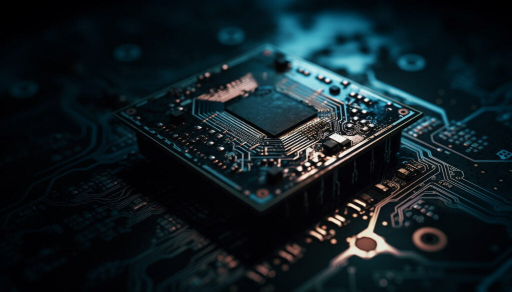
FPGAs are dynamic and adaptable integrated circuits that have completely changed the landscape of digital design. Unlike conventional Application-Specific Integrated Circuits (ASICs), which are fixed in their functioning, FPGAs have the distinct benefit of being very flexible and adaptable since they can be programmed and reprogrammed to carry out a variety of functions.
An FPGA’s extraordinary capabilities are a result of the several interconnected parts that make up its core. This blog will take you on a tour into the complex world of FPGAs as we reveal the mysteries of these electronic powerhouses’ inner workings.
We will begin by looking at the basic parts that make up an FPGA. An FPGA’s building parts, known as configurable logic blocks (CLBs), allow for the implementation of sophisticated logic operations. We’ll find flip-flops and look-up tables (LUTs) that provide sequential operations and logic manipulation inside each CLB. These parts are what really make the FPGA programmable.
Basic Components of an FPGA
Field-Programmable Gate Arrays (FPGAs) are complex integrated circuits that contain various components working together to provide programmable functionality. Understanding the basic components of an FPGA is crucial for comprehending its inner workings and harnessing its potential. In this section, we will delve into the fundamental elements that constitute an FPGA.
- Configurable Logic Blocks (CLBs):
Configurable logic blocks are the primary building blocks of an FPGA. They consist of a combination of look-up tables (LUTs) and flip-flops that can be configured to implement desired logic functions.
- Functionality and Structure of CLBs:
CLBs provide the capability to implement a wide range of digital logic functions. Each CLB typically contains multiple LUTs and flip-flops interconnected through a programmable routing fabric.
- Look-Up Tables (LUTs):
LUTs are programmable lookup tables that store the truth table for a specific logic function. They can be configured to implement various combinational logic functions, such as AND, OR, NOT, and XOR.
- Flip-Flops:
Flip-flops, also known as registers, are storage elements used to hold data values. They can be configured to store and synchronize data within the FPGA design.
- Programmable Interconnects:
Programmable interconnects provide the means to establish connections between different CLBs, I/O pins, and other components within the FPGA.
- Interconnect Structure and its Role:
The interconnect structure consists of a network of wires and switches that enable the routing of signals between different components. It allows for the creation of custom connections to implement specific designs.
- Switch Matrix and Routing Resources:
The switch matrix serves as a routing resource, allowing signals to be directed between different interconnect points. It comprises a collection of programmable switches that can be opened or closed to establish or break connections.
- Configuring Interconnects for Desired Connectivity:
Through configuration, the interconnects can be programmed to establish connections according to the desired circuit layout. This flexibility enables the implementation of complex and customized designs.
Configuration and Programming
- Introduction to FPGA Configuration
- Volatile versus Non-volatile Configuration:
FPGAs can be configured either in a volatile or non-volatile manner. Volatile configuration involves loading the configuration data every time the FPGA powers up, while non-volatile configuration retains the configuration even when power is removed.
- Configuration Storage Elements (Configuration Cells):
FPGAs use configuration cells to store the configuration data that defines the behavior of the logic blocks and interconnects. These cells are typically implemented using flip-flops or static random-access memory (SRAM) cells.
- Programming Methods for FPGAs
- SRAM-based Configuration:
SRAM-based FPGAs are the most common type. They store the configuration data in SRAM cells, which are volatile and require reprogramming each time the device powers up. SRAM-based FPGAs offer flexibility as they can be reprogrammed on-the-fly, allowing for rapid prototyping and design iteration.
- PROM-based Configuration:
Some FPGAs utilize programmable read-only memory (PROM) cells for configuration storage. PROM-based FPGAs are non-volatile, meaning the configuration remains intact even after power cycles. However, PROM-based FPGAs lack the reconfigurability of SRAM-based ones, as the configuration data is fixed during the manufacturing process.
- Flash-based Configuration:
Flash-based FPGAs combine the benefits of both SRAM-based and PROM-based devices. They offer non-volatility like PROM-based FPGAs but also provide the ability to reprogram the configuration like SRAM-based FPGAs. This flexibility makes flash-based FPGAs suitable for applications requiring both long-term configuration retention and dynamic reprogramming.
- Overview of Programming Tools and Languages
- Hardware Description Languages (HDLs):
HDLs, such as VHDL or Verilog, are commonly used to describe the functionality and behavior of the digital circuits implemented within an FPGA. HDLs allow designers to specify the interconnections and logic functions that make up the FPGA design.
- Integrated Development Environments (IDEs):
IDEs provide a comprehensive toolset for FPGA development, including design entry, synthesis, simulation, and programming. Popular FPGA IDEs include Xilinx ISE/Vivado, Intel Quartus Prime, and Lattice Diamond.
- Programming and Configuration Interfaces:
FPGAs are typically programmed and configured using specialized hardware devices such as programmers, JTAG (Joint Test Action Group) interfaces, or USB-based platforms. These interfaces enable communication between the development environment and the FPGA device.
Conclusion
In conclusion, working with Field-Programmable Gate Arrays (FPGAs) requires configuration and programming on a basic level. To fully take use of FPGAs’ flexibility and power while developing digital circuits, one must have a thorough understanding of how they are set up and programmed.
These ideas give designers the ability to alter FPGA behavior and make their designs come to life, whether it’s by deciding between volatile and non-volatile configuration, investigating various programming techniques like SRAM-based, PROM-based, or flash-based, or by using programming tools and languages like HDLs and IDEs.
Engineers may maximize the functionality of these adaptable devices and develop cutting-edge solutions for a variety of applications by learning about FPGA configuration and programming.


")